A PCB is a structure containing electrical circuitry made up of embedded metal wires (traces) and larger areas of metal (planes). The standard dielectric base used in many PCB boards is FR4, a flame-resistant composite of woven fiberglass cloth and epoxy resin, whereas the metal traces and planes for the circuitry are usually composed of copper. Electronic components are installed on the top or bottom layers of the board onto metal pads. PCBs can be a single layer, double layer, or multi-layer.
PCBs are an enabling technology for many advanced research projects. Specialized PCBs are used for various purposes, including wearables, advanced sensor systems, RF and microwave circuits, embedded computers, biomedical research, robotics, etc. The complexity and the number of interconnects of modern electronic components such as embedded microcontrollers and sensor chips continue to increase while the size of the components continues to shrink, making them harder to work with.
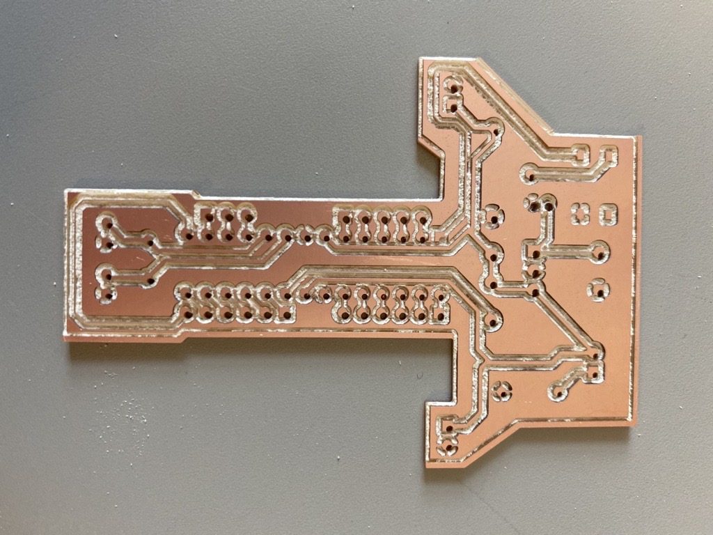
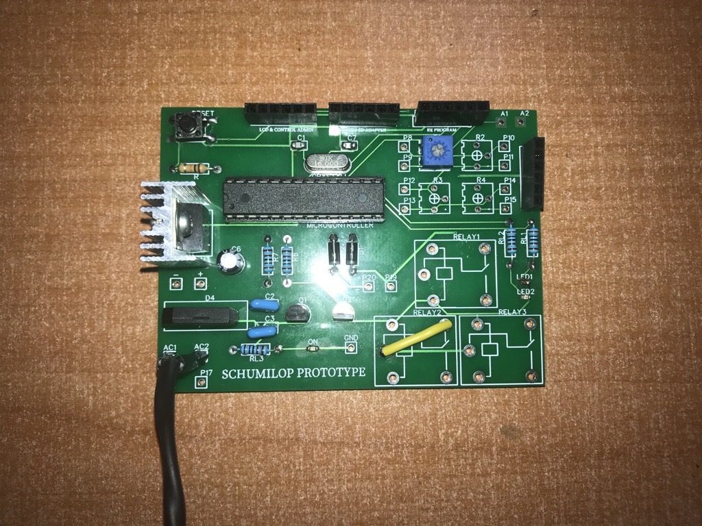
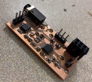
PCB prototyping usually requires multiple iterations. CAPDM can assist you to design your PCB layouts and mill a prototype for your basic research purpose. CAPDM can help you to outsource the design for commercial PCB fabrication. CAPDM can assist you to install components on your PCB boards.